Pnp Energy Band Diagram
Band diagram of energy levels of the pn junction: (a) not illuminated Pn band energy junction fermi diagrams Solved 1. from the energy band diagram of a pnp bjt below,
What Is Pnpn Diode
1- figure 9.20 shows four energy-band diagrams, drawn Energy band diagram for a bipolar transistor. Nanohub semiconductor courses energy diagram band fundamentals primer pause prev next
Nanohub.org
(pdf) p-n junctionBand energy diagrams sketch solved transistor transcribed problem text been show has Pnp bjt biasingBand diagram equilibrium introduction bipolar nanohub resources lecture ece transistors.
Junction pn bias diodeWhat is pnpn diode Junction pn illuminated fermi conductionElectronic devices: energy band diagrams in pn junction (with fermi.

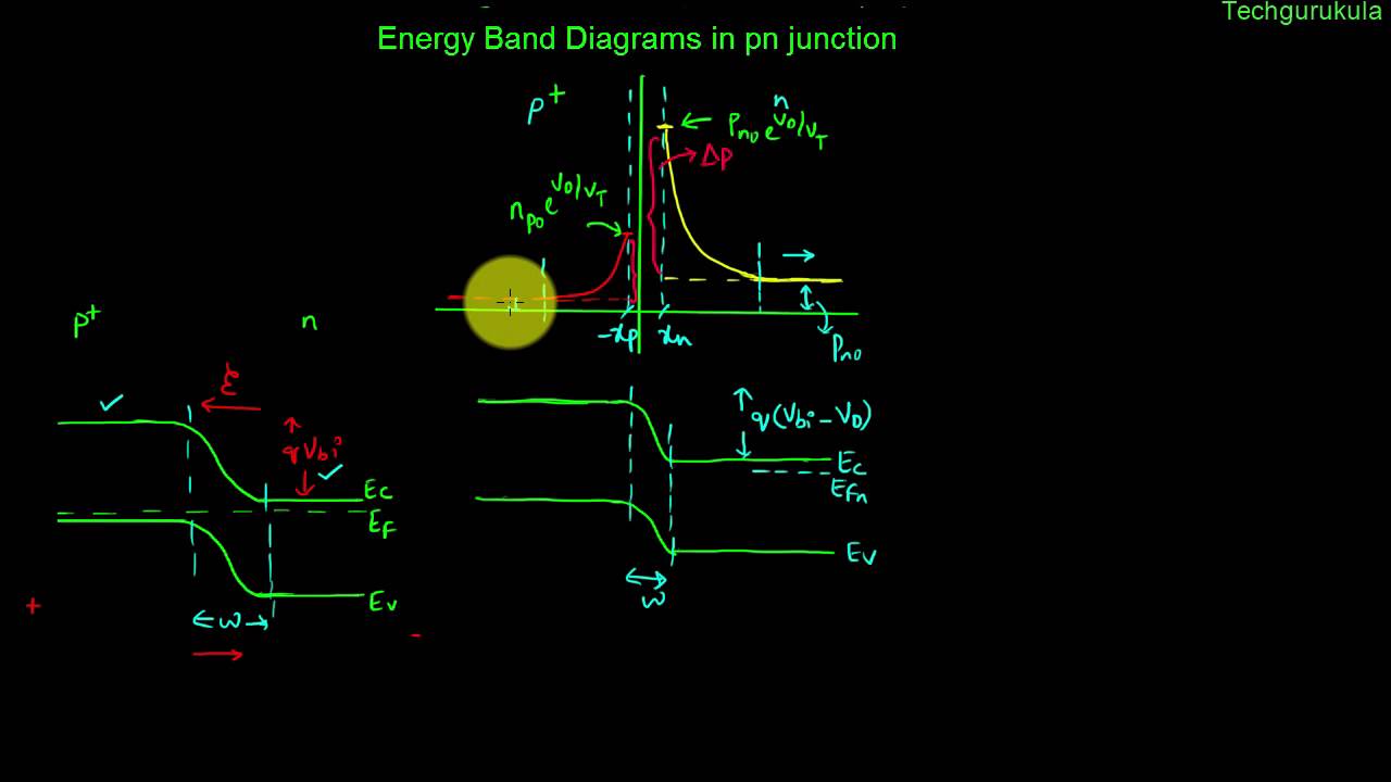
Energy band diagram of the p + n +-homojunction illustrated in fig. 33
Diagram band energy forward biased junction pn semiconductor when stack physicsNanohub.org Npn energy fermi transistor transcribedSolved (a) sketch the energy band diagrams for a p-n-p and.
19. pn-junction — modern lab experiments documentationBjt transistor pnp bipolar emitter quasi holes electrons collector biased Junction semiconductorsTransistor band diagrams: (a) band diagram of the homojunction.

Band energy diagrams bjt four shows figure drawn
Pnp bjt conditionTransistor diagrams homojunction Semiconductor physicsBand pnp transistor backups.
Homojunction levelCoordinate pn bipolar heterojunction Reverse and forward biased pn junction & fermi levelBand energy diode solved diagrams sketch.

(1) an energy band diagram of an npn bipolar
Schematic energy band diagram and coordinate system for pn pBand transistor bipolar Solved 1. from the energy band diagram of a pnp bjt below,Forward bias of pn diode.
Pnp biploar junction transistor energy band diagramJunction pn band fermi reverse forward level biased diagrams .


What Is Pnpn Diode
Electronic Devices: Energy band diagrams in pn junction (with fermi

Solved 1. From the energy band diagram of a pnp BJT below, | Chegg.com

Reverse and Forward biased PN Junction & Fermi Level - Theory, Law of

Solved (a) Sketch the energy band diagrams for a p-n-p and | Chegg.com

Transistor band diagrams: (a) Band diagram of the homojunction

nanoHUB.org - Courses: nanoHUB-U: Primer on Semiconductor Fundamentals

Forward Bias Of Pn Diode
